Semiconductors are materials whose electrical conductivity can be controlled. That simple property allows engineers to make components that switch, amplify, rectify, sense, emit light, and convert electrical energy. Silicon remains the main material for a large share of electronic devices, but compound and wide-bandgap materials now serve applications where frequency, voltage, temperature, optical performance, or power efficiency matters more than material cost alone.
For a purchasing manager or engineer, “semiconductor” is not a sufficient description for a purchase order. A diode, MOSFET, photodiode, microcontroller, and RF power amplifier may all be semiconductors, yet each has different specifications, packaging, lifecycle risks, and inspection needs. This guide explains the major semiconductor types and materials, then connects them to practical component sourcing.
What Is a semiconductor?
Semiconductor definition
A semiconductor is a material with electrical conductivity between that of a good conductor and an insulator. Its conductivity can be changed by adding controlled impurities, applying an electric field, changing temperature, or exposing it to light. Silicon is the most widely used example. Germanium, gallium arsenide, indium phosphide, gallium nitride, and silicon carbide are also used for specific device requirements.
The material becomes useful when it is formed into a device structure. A p-n junction can produce a diode or photodiode. Carefully arranged regions, oxides, and metal contacts can produce a transistor. Many transistors and other structures can then be fabricated on one die to create an integrated circuit.
How semiconductors differ from conductors and insulators
Conductors such as copper have many mobile charge carriers, so current flows easily. Insulators such as glass strongly resist current under normal conditions. A semiconductor sits between these extremes. Its behavior can be adjusted during manufacturing and, in a finished device, controlled by voltage, light, temperature, or magnetic conditions.
That controllability is the important distinction. It lets a circuit turn current on and off, regulate a voltage, detect light, process a signal, or convert power with a defined efficiency. The National Institute of Standards and Technology describes semiconductors such as silicon as materials with tunable electrical conductivity and identifies them as the basis of complex integrated circuits used in communications, computing, healthcare, and transportation. NIST semiconductor overview
Why semiconductors are essential to modern electronics
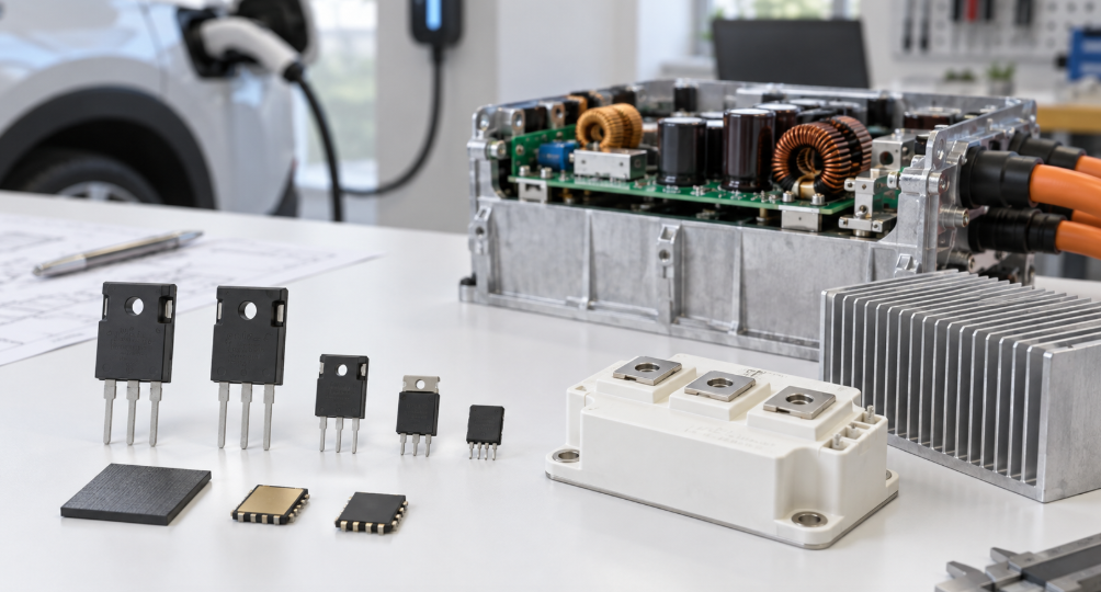
Modern electronics use semiconductors at several levels. Discrete devices protect and control current. Analog ICs condition signals and manage power. Digital ICs perform logic and memory functions. Optoelectronic devices connect electrical and optical systems. Power semiconductors handle energy in chargers, motor drives, solar inverters, and electric vehicles.
For procurement, this variety means the component category alone does not establish suitability. The exact manufacturer part number, suffix, package, temperature grade, and revision must match the design requirement.
How do semiconductors work?
Electrons, holes, and electrical conductivity
In a semiconductor, current is carried by electrons and by holes. An electron is a negatively charged carrier. A hole is the absence of an electron in a crystal structure and behaves as a positive charge carrier. The movement and concentration of these carriers determine how the material responds to an applied voltage.
The crystal is modified through doping. Doping adds a controlled amount of another element to change the available carriers. The result is not simply a material that conducts more or less. It creates regions with different electrical behavior, which engineers use to build junctions, channels, gates, and other device structures.
Intrinsic and extrinsic semiconductors
An intrinsic semiconductor is a relatively pure semiconductor whose carrier concentration is determined mainly by the material and temperature. An extrinsic semiconductor has been intentionally doped to change its electrical properties. Most practical semiconductor devices use carefully controlled extrinsic regions rather than an entirely uniform crystal.
The same base material can support different devices because manufacturing controls the location, concentration, and geometry of doped regions. This is one reason a material name alone is not enough to select a component.
N-type and P-type semiconductor materials
N-type material contains donor impurities that provide more free electrons. P-type material contains acceptor impurities that create more holes. When the two regions meet, the resulting p-n junction can conduct differently depending on the applied voltage. That behavior is used in rectifiers, signal diodes, LEDs, photodiodes, and many sensor structures.
In a transistor, additional regions and terminals allow the device to control a larger current or voltage with a smaller input signal. The exact operation depends on the device family, bias conditions, package, and datasheet limits. A substitute must be checked against those limits rather than selected only because it has the same broad device name.
What are the main types of semiconductors?
Discrete semiconductors
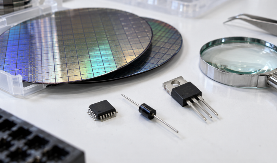
Discrete semiconductors are individual devices supplied as separate components. Common examples include:
- Diodes for rectification, protection, clamping, switching, and signal detection.
- Rectifiers for converting AC to DC in power supplies and chargers.
- Transistors for switching, amplification, regulation, and power control.
- MOSFETs and IGBTs for motor drives, converters, inverters, and other power stages.
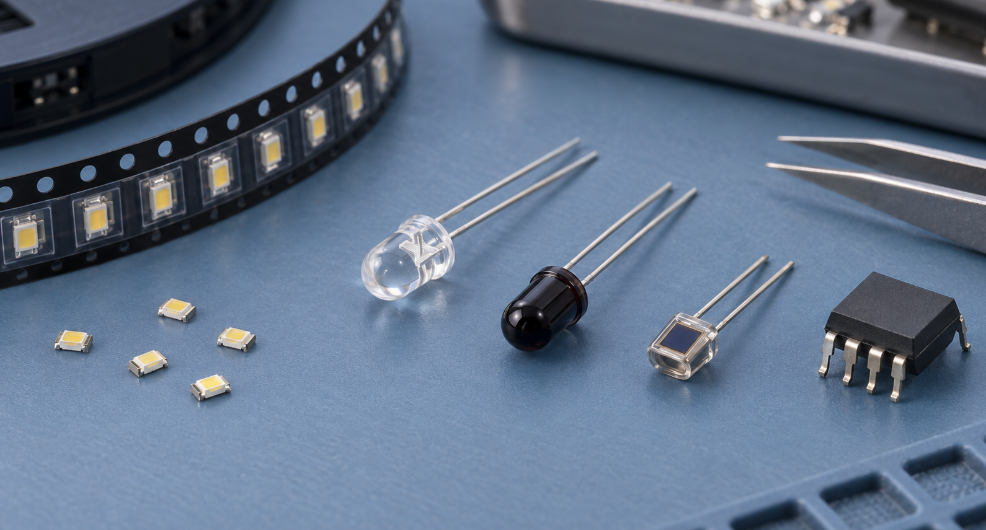
- LEDs, photodiodes, laser diodes, and other optoelectronic components.
When sourcing a discrete device, check the electrical rating, switching behavior, thermal path, package, pinout, marking, and mounting requirements. Two components can look similar while having different gate thresholds, capacitances, recovery behavior, thermal resistance, or safe operating areas.
Integrated circuits
Integrated circuits combine many semiconductor structures on one die. They include microcontrollers, microprocessors, memory devices, analog ICs, power-management ICs, interface devices, sensors, and application-specific ICs.
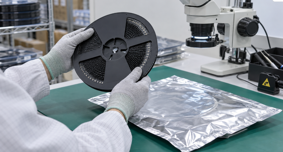
IC procurement adds several checks. Confirm the full ordering code, memory density or interface version where relevant, package suffix, temperature grade, lead finish, packing method, and lifecycle status. For programmable devices, software and configuration compatibility also matter. A pin-compatible alternate may still require engineering validation.
Power, logic, analog, and mixed-signal semiconductors
Power semiconductors are selected around voltage, current, switching frequency, conduction loss, switching loss, thermal resistance, and protection behavior. Logic devices process binary states. Analog devices handle continuous signals such as voltage, current, temperature, and pressure. Mixed-signal ICs combine analog and digital functions, often with converters, interfaces, clocks, and embedded control.
The categories overlap. A power-management IC may contain analog control, digital monitoring, protection logic, and a switching stage. For a BOM review, group parts by function and risk rather than assuming every IC can be evaluated by the same checklist.
What materials are used in semiconductor devices?
| Material family | Typical strengths | Common application direction | Buyer check |
|---|---|---|---|
| Silicon | Mature processing, broad device range, established supply base | Logic, memory, analog, sensors, and conventional power devices | Exact process, package, rating, lifecycle, and source |
| Germanium | Useful material properties in selected devices and research areas | Specialized and legacy applications | Confirm current availability and the exact device specification |
| GaAs and InP | High-frequency or optoelectronic performance in selected designs | RF, microwave, laser, and fiber-optic systems | Verify frequency, optical parameter, package, and qualification |
| SiC and GaN | Wide-bandgap behavior for high-power, high-frequency, or high-temperature designs | EV power conversion, chargers, RF, data-center, and industrial power | Check dynamic ratings, gate drive, thermal design, and application qualification |
Silicon and germanium
Silicon remains dominant because it combines useful electrical properties with a mature manufacturing ecosystem and a wide range of device structures. It is used in logic, memory, analog circuits, sensors, and many power devices. Germanium is less common in mainstream component sourcing but remains relevant in selected semiconductor, infrared, and specialized applications.
Compound semiconductors such as GaAs and InP
Compound semiconductors combine elements from different groups of the periodic table. Gallium arsenide and indium phosphide are used when high-frequency, optical, or other material properties justify their specialized manufacturing and supply considerations. A buyer should not treat a GaAs or InP part as a generic replacement for a silicon device. Frequency range, optical wavelength, package, thermal behavior, and system qualification may all change.
Wide-bandgap materials such as SiC and GaN
Silicon carbide and gallium nitride have wider bandgaps than silicon. They are increasingly used in power and RF applications where switching performance, voltage capability, thermal conditions, size, or efficiency are important. SEMI links their adoption to electric mobility, renewable energy, 5G, smart manufacturing, and robotics. SEMI semiconductor materials overview
SiC is common in high-voltage power conversion, including electric-vehicle inverters and charging systems. GaN is used in high-frequency power conversion and RF designs, including some compact chargers and communications equipment. These devices still require a complete system review. A wider bandgap does not automatically make a device a drop-in replacement. Gate-drive conditions, layout, switching transients, thermal paths, protection, and reliability qualification must be checked by engineering.
What are common semiconductor devices?
Diodes and rectifiers
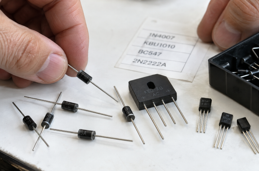
Diodes conduct preferentially in one direction. Rectifier selection may involve forward voltage, reverse voltage, reverse-recovery behavior, leakage, surge current, temperature range, and package thermal performance. Schottky, fast-recovery, TVS, Zener, signal, and bridge rectifiers serve different functions.
Bipolar junction transistors, MOSFETs, and IGBTs
Bipolar junction transistors use current control at the base, while MOSFETs use an electric field at the gate to control the channel. IGBTs combine a MOS gate structure with bipolar conduction characteristics and are used in selected higher-power switching applications. The right choice depends on voltage, current, frequency, conduction loss, switching loss, drive circuit, thermal design, and fault conditions.
For a purchase request, record the full part number and package instead of writing only “MOSFET” or “power transistor.” Check whether the application needs a specific RDS(on), gate charge, avalanche rating, isolation condition, or qualification grade.
LEDs, photodiodes, sensors, and integrated circuits
LEDs convert electrical energy into light. Photodiodes convert incident light into an electrical signal. Sensors use semiconductor structures to detect temperature, pressure, motion, magnetic fields, gas, light, or other conditions. Integrated circuits combine many functions into a compact device.
DuoLink’s optoelectronics category is relevant when a BOM includes LEDs, photodiodes, or related light-based components. Optical parts need additional checks such as wavelength, radiant or luminous output, viewing angle, detector response, package, and temperature behavior.
Where are semiconductors used?
Semiconductors appear in nearly every modern electronic system. In consumer electronics, computers, and data centers, processors, memory, power-management ICs, sensors, interface ICs, and optical devices work together. High-performance computing and data-center equipment also place strong demands on power conversion, thermal management, memory, and high-speed interconnects.
Automotive electronics use microcontrollers, sensors, power devices, communication ICs, LED drivers, motor-control devices, and protection components. Electric vehicles add traction inverters, battery-management systems, onboard chargers, DC-DC converters, and charging infrastructure. Silicon carbide is increasingly associated with high-voltage power conversion, while the final device choice still depends on the vehicle platform and qualification requirements. The U.S. Department of Energy describes silicon-based devices as the established foundation of vehicle power electronics and identifies SiC and GaN as important wide-bandgap research areas. DOE power electronics research
5G communications use RF front ends, power amplifiers, filters, converters, processors, and optical or wired network components. Industrial automation uses PLCs, motor drives, robotics controls, sensors, relays, and safety-related electronics. Medical equipment, aerospace systems, and defense applications may impose stricter qualification, traceability, environmental, export, or documentation requirements.
DuoLink describes its work as independent electronic-component supply, including semiconductors, ICs, BOM sourcing, inventory inquiries, and hard-to-find parts. Buyers can review the about page and submit a requirement through the DuoLink website. Availability, authenticity, documentation, and suitability still need to be verified for the specific part and application.
How to select and source semiconductor components
Start with the complete part requirement
Provide the manufacturer, full part number, quantity, package, target application, required date code, acceptable alternates, and document requirements. Key specifications may include:
- Voltage, current, power, frequency, gain, or optical parameters.
- Package, pinout, mounting method, and thermal interface.
- Operating temperature, qualification grade, and environmental limits.
- Lifecycle status, revision, date code, lot code, and packing format.
- RoHS, REACH, customer-specific, automotive, medical, aerospace, or other compliance needs.
Do not approve an alternate from a short parametric match alone. Form, fit, and function may also depend on transient behavior, firmware, thermal impedance, switching losses, optical response, or qualification history.
Check manufacturer, part number, date code, authenticity, and lifecycle
Compare the offered part with the current manufacturer datasheet and product-status information. Review the full suffix, package drawing, marking convention, and any PCN or PDN information. Ask whether the offered stock is factory sealed, repacked, mixed lot, supplier held, or already allocated to another order.
Before shipment, request current photos of reels, trays, labels, date codes, lot codes, and packaging when the risk or value justifies it. At receiving, compare labels and top markings, inspect leads or balls, check for oxidation or surface rework, and quarantine mismatches. Visual inspection can identify warning signs, but it does not prove authenticity by itself. Higher-risk applications may require electrical testing, X-ray, XRF, decapsulation, or another defined inspection plan approved by quality and engineering.
When to use BOM sourcing
BOM sourcing is useful when a project contains many semiconductor families, several lines are obsolete or allocated, or the buyer needs one process for part-number review, stock inquiry, quotation, and document collection. It can also help separate low-risk active parts from sole-source, shortage, end-of-life, or hard-to-find lines.
DuoLink’s BOM procurement support can be considered for that workflow. Send the BOM with manufacturer preferences, quantities, target dates, approved alternates, date-code limits, and required documents. The buyer should still define the acceptance criteria and obtain engineering approval for any replacement.

Conclusion
Semiconductors are controllable electronic materials used to build diodes, transistors, optoelectronic devices, sensors, power stages, and integrated circuits. Silicon remains the broadest platform, while GaAs, InP, SiC, and GaN serve designs with specific frequency, optical, voltage, temperature, or efficiency requirements.
For an overseas purchase, the useful question is not only “What type of semiconductor is this?” It is also “Which exact part meets the design, documentation, lifecycle, and quality requirements?” Confirm the full part number, specifications, packaging, source evidence, lot and date-code needs, and alternate approval before placing the order.
DuoLink Electronics is an independent electronic-component supplier supporting integrated circuits, semiconductors, passive components, connectors, BOM sourcing, part-number lookup, inventory inquiry, and hard-to-find component sourcing. Buyers can submit the manufacturer, part number, quantity, application, date-code requirement, and documentation needs for a specific sourcing review.
Frequently asked questions
Is silicon still the main semiconductor material?
Yes. Silicon remains widely used for logic, memory, analog ICs, sensors, and many power devices. GaN, SiC, GaAs, and InP are selected when their properties better fit a particular power, frequency, optical, thermal, or application requirement.
Are GaN and SiC direct replacements for silicon devices?
Usually not. The replacement must be checked for voltage and current ratings, switching behavior, gate drive, thermal design, package, protection, layout, reliability, and system qualification. Engineering approval is required before changing a qualified design.
What information should I send when sourcing a semiconductor?
Send the manufacturer, complete part number and suffix, package, quantity, application, target delivery date, acceptable alternates, date-code limits, and required compliance or traceability documents. A full BOM is useful when several component families need to be reviewed together.
Can visual inspection prove that a semiconductor is genuine?
No. Markings, labels, packaging, and lead condition can reveal warning signs, but they are screening evidence. The inspection scope should match the component risk and may include documentation review, electrical testing, X-ray, XRF, or other approved methods.
Can DuoLink source obsolete or hard-to-find semiconductor parts?
DuoLink presents itself as an independent supplier supporting hard-to-find component sourcing, inventory inquiries, and BOM support. Availability, source, authenticity evidence, and documentation must be confirmed for each requested part before purchase.


 English
  German
  Spanish
  French
  Chinese
  Italian