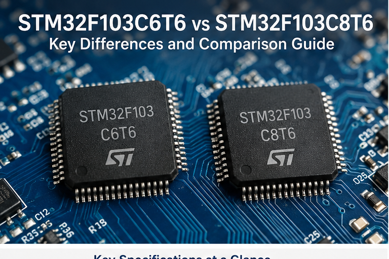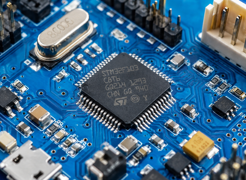
The STM32F103C8T6 has been on engineers’ BOMs for years, yet it still creates small but expensive mistakes. The part name looks simple. Once you start checking Flash size, package, alternate pin functions, USB/CAN sharing, temperature suffixes, and possible replacements, the details matter much more than the headline “72 MHz Cortex-M3 MCU.”
From a sourcing point of view, I usually look at this device from two directions. The engineer wants to know whether the STM32F103C8T6 has enough memory, GPIO, timers, ADC channels, and communication interfaces. The purchasing team needs to know whether the quoted part is the exact device approved in the BOM. Those two questions should be answered together.
This guide explains the STM32F103C8T6 pinout, specifications, peripheral functions, applications, related STM32F1 devices, and the checks worth making before you place an order. If you are still deciding between MCU families or memory sizes, our guide on how to choose a microcontroller for an embedded system gives a broader selection framework.
1. What Is the STM32F103C8T6?
The STM32F103C8T6 is a 32-bit microcontroller from STMicroelectronics’ STM32F1 performance line. It uses an Arm Cortex-M3 core and runs at up to 72 MHz. The C8 version provides 64 KB of embedded Flash and 20 KB of SRAM. The T package code identifies an LQFP package, while the C pin-count code indicates 48 pins.
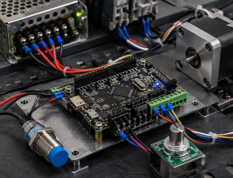
It sits in an interesting middle ground. You get more processing capability and peripheral flexibility than many basic 8-bit MCUs, but the device is still straightforward enough for control boards, sensor interfaces, motor-control designs, communication nodes, and general embedded hardware.
The STM32F103 family supports USB, CAN, ADC, PWM, timers, UART/USART, SPI, and I²C. For the 48-pin STM32F103Cx devices, ST specifies 37 GPIOs, two 12-bit ADCs with 10 external channels, three USARTs, two SPI interfaces, two I²C interfaces, USB, and CAN.
That mix explains why the STM32F103C8T6 appears in many embedded products. It can read analog sensors, control motors, communicate with several external devices, run a real-time control loop, and still leave room for status LEDs, switches, interrupts, and diagnostic interfaces.
STM32F103C8T6 at a Glance
One detail is worth remembering before going any deeper: STM32F103C8T6 officially means 64 KB Flash. You may see development boards, software tools, or third-party listings that suggest more memory. For production design and purchasing, use the manufacturer-defined part number rather than assuming extra Flash is guaranteed. ST’s ordering scheme defines the “8” memory code as 64 KB and “B” as 128 KB.
That distinction becomes useful later when comparing the C8 with the STM32F103CBT6.
2. STM32F103C8T6 Key Features and Specifications
For most engineers, the real value of the STM32F103C8T6 comes from the balance between CPU performance, memory, analog functions, timers, and communication peripherals.
| Specification | STM32F103C8T6 |
|---|---|
| Manufacturer | STMicroelectronics |
| MCU Family | STM32F1 Performance Line |
| CPU Core | 32-bit Arm Cortex-M3 |
| Maximum CPU Frequency | 72 MHz |
| Flash Memory | 64 KB |
| SRAM | 20 KB |
| Package | LQFP-48, 7 × 7 mm |
| GPIO | 37 |
| ADC | 2 × 12-bit ADCs |
| External ADC Channels | 10 |
| General-Purpose Timers | 3 × 16-bit |
| Advanced-Control Timer | 1 × 16-bit |
| USART | 3 |
| SPI | 2 |
| I²C | 2 |
| CAN | CAN 2.0B Active |
| USB | USB 2.0 Full Speed |
| DMA | 7 channels |
| Debug | SWD and JTAG |
| Operating Supply | 2.0–3.6 V |
| Temperature Range for T6 | –40°C to +85°C |
| Additional Functions | RTC, watchdogs, CRC, 96-bit unique ID |
These specifications follow ST’s medium-density STM32F103 documentation.
The 72 MHz clock gets most of the attention, but memory and peripherals usually decide whether this MCU fits a real design.
64 KB of Flash is enough for many control, sensing, communication, and embedded user-interface tasks. Firmware with large protocol stacks, multiple middleware layers, file systems, graphics, or frequent feature expansion can reach that limit faster than expected. If your code is already close to the boundary during prototype development, moving to the 128 KB STM32F103CBT6 can be cleaner than designing around unused space that is not part of the official C8 specification.
20 KB of SRAM also needs to be considered early. Buffers for serial communication, USB traffic, sensor data, RTOS tasks, and local data structures all compete for the same RAM.
The STM32F103C8T6 includes a 7-channel DMA controller. DMA lets supported peripherals move data without requiring the CPU to handle every byte or ADC sample directly. This can make a real difference in applications that collect repeated ADC data, receive serial streams, or drive peripherals while the processor handles control logic.
Clock flexibility is another useful part of the design. The MCU includes an internal 8 MHz RC oscillator and a 40 kHz internal low-speed RC source. It can also use an external 4–16 MHz high-speed crystal and a 32.768 kHz low-speed crystal for RTC-related functions.
3. Understanding the STM32F103C8T6 Pinout
Searching for an “STM32F103C8T6 pinout” usually means more than finding a 48-pin drawing. The real question is: which pins can I safely assign to each function without creating conflicts later?
The STM32F103C8T6 uses the 48-pin LQFP configuration. ST’s pinout shows power, oscillator, reset, boot, GPIO, analog, communication, timer, and debug functions distributed across the package.
The trap is pin multiplexing. A pin such as PA11 is not simply GPIO number 11. It can also serve USB, CAN, timer, or USART-related functions depending on configuration. Your schematic may appear to have enough pins until two required peripherals try to use the same physical connection.
GPIO, Power, and Communication Pins
The main digital I/O groups are PA0–PA15, PB0–PB15, and PC13–PC15, although several pins have dedicated startup, oscillator, or debug roles and cannot simply be treated as unrestricted GPIO.
Power connections deserve close attention. VDD pins supply the digital section, while VSS pins provide digital ground. VDDA and VSSA support the analog domain. If you plan to use the ADC with meaningful accuracy, analog supply layout, grounding, decoupling, and signal routing matter just as much as configuring the ADC registers.
VBAT provides backup-domain power for the RTC and backup registers. This is useful when the main supply may be removed while timekeeping needs to continue.
PD0 and PD1 are used as the high-speed external oscillator input and output in the LQFP-48 version. PC14 and PC15 support the low-speed 32.768 kHz oscillator. PC13 also has RTC/tamper-related functionality.
BOOT0 is another pin I always check when reviewing a board. PB2 can act as BOOT1 in the STM32F103 medium-density device. Their startup state affects the boot path, so resistor configuration around these pins should match the intended programming and production process.
Communication pins need the same planning.
USART1 normally uses PA9 for TX and PA10 for RX. SPI1 commonly uses PA4 through PA7 for NSS, SCK, MISO, and MOSI. I²C1 can use PB6 and PB7 for SCL and SDA. The device also offers alternate remapping options for several peripherals.
One pin conflict deserves special attention: PA11 and PA12 are the default CAN RX/TX pins and also USB DM/DP pins. If your product needs both USB and CAN, you cannot treat those functions as independent when planning the default pin map. CAN can be remapped to PB8 and PB9, which can solve the conflict when the rest of the board configuration supports that choice.
This is the kind of detail that is easier to fix during schematic design than after PCB routing.
ADC, PWM, and Debug Pins
For the STM32F103C8T6, the main external ADC inputs are found on PA0–PA7 and PB0–PB1, giving 10 available channels in the 48-pin Cx configuration. These pins can carry other alternate functions too, so analog channel planning should happen before the remaining GPIO is assigned.
The two ADC units are 12-bit converters. ST specifies conversion capability down to around 1 µs under the stated clock conditions. The input conversion range extends from 0 V to the analog supply range, up to 3.6 V in the family specification.
Do not read “almost all I/Os are 5 V tolerant” as permission to apply 5 V to every STM32F103C8T6 pin. The datasheet identifies 5 V-tolerant digital pins separately, while several analog-capable and dedicated pins do not carry that FT designation. Check the exact pin before connecting a 5 V logic source.
For PWM and timing, the MCU includes three general-purpose 16-bit timers and one advanced-control timer. The advanced timer is especially useful for motor-control work because it supports features such as complementary PWM outputs, dead-time generation, and emergency-stop functions. General-purpose timers can also handle input capture, output compare, pulse counting, PWM, and quadrature encoder signals.
Debugging normally uses PA13 for SWDIO and PA14 for SWCLK. Full JTAG also occupies PA15, PB3, and PB4. If you only use SWD, some of those JTAG pins can be released for other functions after the debug configuration is set. I still prefer keeping SWD accessible on production boards when field programming, firmware recovery, or engineering diagnostics may be needed.
4. Communication Interfaces and Peripheral Functions
The STM32F103C8T6 becomes much easier to evaluate when you connect each peripheral to a real design requirement.
USART works well for debugging terminals, GNSS modules, serial sensors, wireless modules, industrial serial links, and communication with another MCU. RS-232 and RS-485 systems still require the proper external physical-layer transceiver.
SPI fits higher-speed local peripherals such as external Flash, displays, high-speed sensors, ADCs, DACs, and communication controllers. The STM32F103C8T6 provides two SPI interfaces capable of up to 18 Mbit/s according to ST’s specification.
I²C is useful when several lower-speed devices need to share two signal lines. Temperature sensors, EEPROMs, RTC devices, small displays, battery monitors, and other board-level ICs often use this interface.
CAN 2.0B makes the MCU suitable for distributed control networks in machines, automation equipment, and vehicle-related systems. The STM32 contains the CAN controller, but your board still needs an external CAN transceiver for the physical bus connection.
USB 2.0 Full Speed allows the MCU to communicate directly with a USB host when the hardware and clock design meet the interface requirements. This can support device communication, configuration, data transfer, and other embedded USB functions.
The ADCs, DMA, timers, interrupts, and communication peripherals can also work together. A typical embedded architecture might let a timer trigger ADC sampling, use DMA to move samples into memory, process the data in firmware, then send selected information through UART, USB, or CAN. That combination often matters more than CPU frequency alone.
If you are selecting MCUs for PLC-related boards, motor controllers, machine interfaces, or sensor nodes, our industrial automation applications section provides more context around component requirements in industrial systems.
5. Common Applications of the STM32F103C8T6
The STM32F103C8T6 works best when the application fits its memory size and pin count. It should not be chosen simply because the part is familiar.
| Application | Why the STM32F103C8T6 Fits |
|---|---|
| Industrial Control Systems | Timers, ADC, CAN, USART, GPIO, watchdogs, and interrupt support fit many control-board functions |
| Motor Control | Advanced PWM timer, dead-time control, ADC inputs, and encoder support are useful for motor-drive control |
| Sensors and Data Acquisition | 12-bit ADC, DMA, SPI, I²C, and USART support sensor collection and data transfer |
| Robotics | PWM, encoder inputs, serial communication, ADC, and GPIO can handle actuators and sensor interfaces |
| IoT Edge Devices | The MCU can manage local sensing and control while an external Wi-Fi, cellular, LoRa, or other communication module handles connectivity |
| Consumer Electronics | USB, buttons, LEDs, displays, sensors, and serial peripherals can be integrated around one controller |
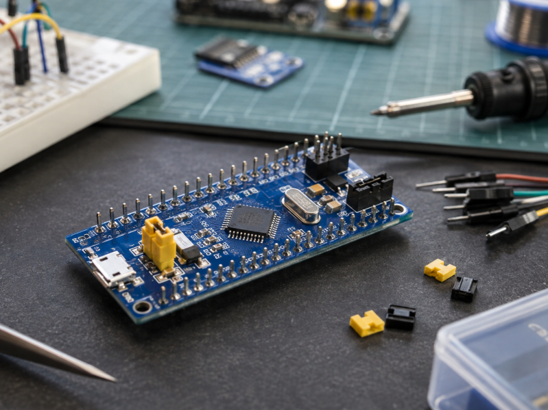
| Embedded Development Boards | The 48-pin package offers enough accessible peripherals for learning, prototyping, firmware development, and testing |
ST itself lists motor drives, application control, medical and handheld equipment, industrial systems, PLCs, inverters, PC peripherals, alarm systems, and HVAC equipment among the broader uses for the medium-density STM32F103 family.
Application fit still depends on the finished system. An industrial controller may need CAN and multiple timers but little Flash. A data logger may need more memory. A small HMI can run out of Flash or SRAM long before it runs out of GPIO.
This is why I prefer to select the MCU from the whole peripheral map rather than starting with “72 MHz should be enough.”
6. STM32F103C8T6 vs Similar STM32 Microcontrollers
The STM32F103C8T6, STM32F103CBT6, and STM32F103RCT6 share the Cortex-M3 architecture and a maximum CPU frequency of 72 MHz, but they are not interchangeable in the same way.
| Device | STM32F103C8T6 | STM32F103CBT6 | STM32F103RCT6 |
|---|---|---|---|
| Core | Cortex-M3 | Cortex-M3 | Cortex-M3 |
| Max. Frequency | 72 MHz | 72 MHz | 72 MHz |
| Flash | 64 KB | 128 KB | 256 KB |
| SRAM | 20 KB | 20 KB | 48 KB |
| Package | LQFP-48 | LQFP-48 | LQFP-64 |
| GPIO | 37 | 37 | 51 |
| ADC | 2 | 2 | 3 |
| External ADC Channels | 10 | 10 | 16 |
| USART | 3 | 3 | 5 |
| SPI | 2 | 2 | 3 |
| I²C | 2 | 2 | 2 |
| USB | Yes | Yes | Yes |
| CAN | Yes | Yes | Yes |
| DAC | No | No | 2 × 12-bit |
ST defines the STM32F103CB as the 128 KB version of the same medium-density 48-pin C family. That makes the STM32F103CBT6 the most natural device to investigate when your main problem is C8 Flash capacity. It keeps the LQFP-48 package and the same 37-GPIO class. Firmware memory configuration still needs to be updated and the full design should be revalidated before substitution.
The STM32F103RCT6 is a bigger step. It moves into the high-density STM32F103 family with 256 KB Flash, 48 KB SRAM, 51 GPIOs, three ADCs, more timers, more serial interfaces, two DAC channels, and an LQFP-64 package. This is not a drop-in C8 replacement because the footprint and peripheral map change.
The choice is fairly practical. If the PCB is fixed and firmware mainly needs more Flash, check the CBT6. If the design needs more memory, more I/O, DAC outputs, or a wider peripheral set, the RCT6 may make more sense at the architecture stage.
7. How to Choose and Source the STM32F103C8T6
This is where engineering information becomes purchasing information.
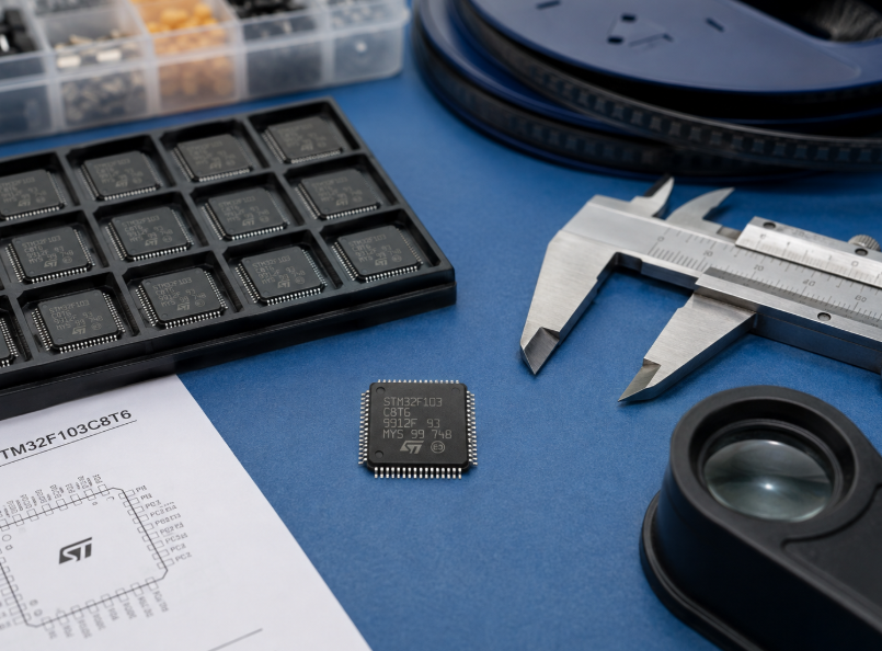
When I review an MCU RFQ, the first thing I want is the complete manufacturer part number. “STM32F103” is not enough. “STM32F103C8” still leaves purchasing details open. STM32F103C8T6 tells you much more.
ST’s ordering code breaks down this way: C = 48 pins, 8 = 64 KB Flash, T = LQFP, 6 = industrial temperature range from –40°C to +85°C. A “TR” suffix identifies tape-and-reel packing.
This part-number check is simple, but it prevents a surprising number of BOM problems. A C8 and CB may look almost identical in a spreadsheet. A T6 and another package suffix can create a physical assembly problem. A temperature suffix can matter once the end product leaves a laboratory environment.
Next, confirm that the documentation matches the actual quoted part. Check manufacturer marking, package type, packing method, labels, lot or date information, lifecycle status, and traceability information available from the supply channel.
Photos are useful, but I do not treat a clean top marking as proof of authenticity. Procurement teams should judge the complete supply chain. Depending on risk level, order quantity, end application, and sourcing channel, incoming inspection may include packaging and label review, marking inspection, electrical testing, X-ray analysis, or more detailed laboratory work.
Date code needs sensible treatment too. An older date code does not automatically mean a component is unsuitable, just as a recent date code does not prove authenticity. Storage history, packaging condition, moisture handling, traceability, and the customer’s own manufacturing requirements should be considered together.
Compliance documentation also needs to match the destination market and finished product requirements. For equipment sold into the EU, buyers may need material information related to the EU RoHS restrictions on hazardous substances. The European Commission states that RoHS restricts ten hazardous substances in electrical and electronic equipment.
REACH is a separate regulatory framework. When your customer or compliance team asks about substances of very great concern, the ECHA Candidate List is the appropriate official reference point.
A component material declaration can support downstream compliance work, but it should not be treated as proof that the complete finished product automatically complies with every applicable regulation. Product-level compliance still depends on the full bill of materials, manufacturing process, market, and applicable legal scope.
For ST parts, you can also review our STMicroelectronics component selection when checking related MCUs and electronic components. The key is still the same: match the exact MPN to the engineering requirement before accepting a sourcing alternative.
Conclusion
The STM32F103C8T6 remains a practical 32-bit microcontroller for control systems, sensors, motor-control designs, robotics, embedded communication, and many general-purpose MCU projects. Its Cortex-M3 core, 72 MHz clock, 64 KB Flash, 20 KB SRAM, 37 GPIOs, ADCs, timers, USB, CAN, SPI, I²C, and USART interfaces give engineers a useful set of functions in a compact LQFP-48 package.
The part becomes easier to use once you stop looking at each feature separately. Check pin multiplexing before PCB routing. Watch the PA11/PA12 USB and CAN overlap. Keep the official 64 KB Flash specification in mind. Decide whether the 20 KB SRAM leaves enough headroom for future firmware. When you move from prototype to purchasing, verify the entire STM32F103C8T6 part number rather than ordering from a shortened description.
If you are also sourcing electronic components, Duolink Electronics is an independent electronic components supplier providing integrated circuits, semiconductors, passive components, connectors, and other electronic parts. We support BOM sourcing, part-number checking, inventory inquiries, and sourcing for difficult-to-find components. If you have an STM32F103C8T6 requirement or another electronic component on your BOM, you can leave your requirements through our website and contact our team for sourcing support.
Frequently Asked Questions
Is the STM32F103C8T6 a 64 KB or 128 KB Flash MCU?
The official specification for STM32F103C8T6 is 64 KB Flash. In ST’s ordering code, “8” represents 64 KB. The STM32F103CBT6 uses “B” and provides 128 KB. For production designs, do not rely on undocumented extra memory.
Can I replace STM32F103C8T6 with STM32F103CBT6?
The CBT6 is the closest option when you need 128 KB Flash while staying in the 48-pin LQFP STM32F103C family. Check firmware memory settings, peripheral configuration, approved BOM data, and the latest manufacturer documentation before releasing the substitution.
Which pins are used for SWD programming?
PA13 is used for SWDIO and PA14 for SWCLK. Keeping these signals accessible on the PCB makes programming, debugging, and firmware recovery much easier.
Can STM32F103C8T6 use USB and CAN together?
Yes, but pin planning matters. USB uses PA11 and PA12, which are also the default CAN RX and TX pins. CAN can be remapped to PB8 and PB9, allowing both interfaces to be used when the hardware and firmware are designed around that configuration.
What information should I include when requesting an STM32F103C8T6 quotation?
Send the complete MPN, required quantity, packing preference, delivery requirement, acceptable date-code conditions if your project has them, and any traceability, inspection, RoHS, or REACH documentation requirements. For an approved BOM, state whether substitutions are allowed before the supplier proposes another STM32 device.